The Interface
       

Pinouts and cables for telecomms

  home | contacts | site policy    
   

RS 232 connector

 
  MENU

This page describes the V.24 recommendation as set out by CCITT , the following will give you more detailed information regarding pinouts and specific cabling requirements.


CCITT V.24/28       EIA RS-232 (American equivalent)

Most computers,terminals,printers and modems have a familiar connector with either 9 pin D-Type or 25 pin D-Type , if so this connector probably conforms to the CCITT V.24 / RS232 standard. 25way
ISO 2110
This defines the physical shape of the interface connector. It also assigns the V.24 circuits to the  pins on the interface . Normally the terminal side (DTE) will have a male 25 pin D-Type connector and the modem , printer etc...(DCE) has a female 25 pin D-Type socket.( On most PCs the connector is a 9 pin D-Type ).
 
The categories of circuits terminating on these connectors are as follows:
  1. Ground
  2. Data
  3. Control
  4. Timing
The Active Circuits share a common ground on the connector which is why the cable connecting two pieces of equiptment is called "Electrically Unbalanced".
 

CCITT V.28

The V.28 specification details the electrical characteristics of the interface .
The receiving device must recognise a signal of :
  • -3 Volts or less to represent a binary '1' bit (OFF condition).
  • +3 Volts or more to represent a binary '0' bit (ON condition).
The signal at the transmitter should be at least + or - 5 Volts however signals +/-8 Volts to +/- 12 Volts are typical. The region between +3 Volts and -3 Volts is defined as the transition region.
Voltage Graph
 transit voltage
 
The MAXIMUM RECOMMENDED distance between DTE and DCE is 15 Meters. Greater distances are acheivable using high grade cables but it is best to stick to the recommended 15 meters as a maximum. If one uses a longer cable connection it will more than likely experience some interference resulting in errors. However I have personally used a Category 5 twisted pair cable for a 35 Meter circuit and have had no problems so far !

   
CCITT V.1
CCITT V.1 defines the binary equivalents for serial data , the 1 and 0 bits are always represented the same way:
  • 0 = Start = Space = High = Blank =  +3v      =  ON
  • 1 = Stop = Mark   = Low  = Hole   =   -3v      =  OFF
This is easiest remembered using the spoon rule !

S  P  O  O  N

Space  Positive Zero ON


LINKS


CCITT V.24

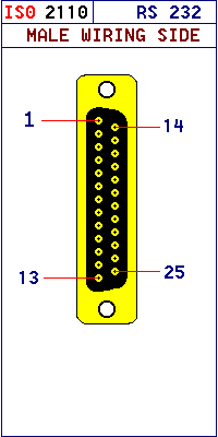
CCITT V.24 defines the functions of the V.28 voltage signals and their category .Each pin on the D-Type ISO 2110 connector is assigned a function and given a number between 100 and 199. The interface signals are always defined with respect to the terminal (DTE) . Transmitted data on pin 2 of the terminal is output on pin 2 of the DTE and goes directly as input on pin 2 of the DCE (modem). The Signal Ground on pin 7 serves as a common reference so that both devices can recognise positive and negative voltages.

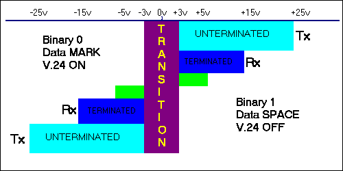
In an asynchronous environment a minimum of 3 connections are required pins 2 Transmit , 3 Receive and pin 7 Ground . A more sophisticated interface will use pin 20 DTR , 6 DSR , 4 RTS ,5 CTS and pin 8 DCD . These signals allow DTE and DCE to keep each other informed of their current status (Handshaking). Asynchronous means that timing/clock is part of the data and not provided separately.

Synchronous circuits have separate timing/clocking sources to synchronise data being transmitted.Depending on the source chosen for clocking pins 15 ,17 or 24 are used.


CCITT V.24 Circuits Explained

101    Protective Ground  

  • Rarely used protective/shield ground extended from DTE to DCE.

102    Signal Ground        

  • Common signal return/ground for all other signals.

103    Transmit Data         

  • Data transmitted out from the DTE.

104    Receive Data          

  • Data receive input to the DTE from modem or other equiptment.

105    Request to Send    

  • When the DTE wishes to send data it turns 105 on , in a full duplex system this circuit is permanently on.

106    Clear to Send         

  • Response 105 by modem (DCE) to indicate modem is ready to send data over the modem link to the distant modem(DCE).

107    Data Set Ready      

  • This circuit indicates that the DCE is connected to line and is a response to the DTE signal DTR (108).

108    DTR / CDSTL          

  • There are two options for this circuit:
  • 108/2 DTR provides the terminal with indirect control over switching the modem to line.An ON condition on this circuit from the DTE informs the DCE that the terminal is ready to operate.This can also be used when the modem has automatic answering facilities.When waiting for a call 108/2 remains ON,then when the RI (125) is turned on the modem is automatically switched to line,the modem turns 107 on.
  • 108/1 CDSTL is used to give the terminal direct control over switching the modem to the telephone line .The call is dialled with 108/1 off and when the call is answered the circuit is turned on by the Terminal (DTE) .The ON condition will connect the modem to line.Turning 108/1 off disconnects the modem from line.

109    Data Carrier Detect  

  • This circuit is turned ON by the DCE to indicate it has received carrier.

111    Data Signalling Rate Selector  

  • Some modems allow different speeds to be selected (1200/75) and when so , this circuit being ON selects the higher rate.

113    Transmit Signal Element Timing  

  • Transmit Signal Element Timing DTE -->  DCE   terminal provides timing.

114    Transmit Signal Element Timing

  • Transmit Signal Element Timing DCE --> DTE modem provides timing . This is the usual usage and it should be noted that only one of 113 or 114 can be used not both!  

115    Transmit Signal Element Timing

  • Receive Signal Element Timing  DCE --> DTE.Clocks the received data on 104 and is derived from the incoming modulated signal and is thus synchronised with the timing at the source transmitting.

118    Transmit Backward Channel Data

  • Equivalent to Transmit Data on 103 DTE --> DCE.

119    Receive Backward Data Channel

  •   Equivalent to Receive Data on 104, DCE --> DTE.

120    Secondary RTS  

  • Secondary Request to Send equivalent to 105, DTE --> DCE.

121    Secondary CTS  

  • Secondary Clear to Send equivalent to 106, DCE --> DTE.

122    Secondary DCD

  •   Secondary Data Carrier Detect equivalent to 109 , DCE --> DTE.

125    Ring Indicator

  • This circuit reacts to an incoming call to the modem ,ie it is on when the ringing current is being sent by an exchange to the modem..

126    Select Transmit Frequency  

  • Designed for old V.21 200/300 baud modems to select which speed this side would use to transmit / modulate its data.

140    Initiate Remote Digital Loop

  • ON requests the remote modem to provide a Digital Loopback if it has this option enabled.

141    Initiate Local Analogue Loop  

  • ON requests the locally connected modem to provide an analog loop.

142    Test Indicator 

  • ON indicates the local modem is in test mode!
 

Connectors and pin designations

PIN V.24 RS-232 DTE- DCE DESCRIPTION
1 101 AA   Protected Ground or shield
2 103 BA diagrams/dtedce.gif (95 bytes) Transmitted Data
3 104 BB ../images/diagrams/dcedte.gif (94 bytes) Receive Data
4 105 CA ../images/diagrams/dtedce.gif (95 bytes) RTS  Request to Send
5 106 CB ../images/diagrams/dcedte.gif (94 bytes) CTS  Clear to Send
6 107 CC ../images/diagrams/dcedte.gif (94 bytes) DSR  Data Set Ready
7 102 AB   Signal Ground    / Common
8 109 CF ../images/diagrams/dcedte.gif (94 bytes) DCD  Data Carrier Detect
9       Positive test voltage (sometimes)
10       Negative test voltage (sometimes)
11 126   ../images/diagrams/dtedce.gif (95 bytes) Select Transmit Frequency   (National use)  V.21 only
12 122 SCF ../images/diagrams/dcedte.gif (94 bytes) Secondary DCD
13 121 SCB ../images/diagrams/dcedte.gif (94 bytes) Secondary CTS
14 118 SBA ../images/diagrams/dtedce.gif (95 bytes) Secondary Transmit
15 114 DB ../images/diagrams/dcedte.gif (94 bytes) Transmit Signal Element Timing (Master)
16 119 SBB ../images/diagrams/dcedte.gif (94 bytes) Secondary Receive
17 115 DD ../images/diagrams/dcedte.gif (94 bytes) Receive Signal Element Timing
18 141   ../images/diagrams/dtedce.gif (95 bytes) Initiate Local Analogue Loop
19 120 SCA ../images/diagrams/dtedce.gif (95 bytes) Secondary RTS
20 108 CD ../images/diagrams/dtedce.gif (95 bytes) 108/1  CDSTL Connect Data Set to line

108/2  DTR      Data Terminal Ready

21 140   ../images/diagrams/dcedte.gif (94 bytes) Initiate Remote Digital Loop
22 125 CE ../images/diagrams/dtedce.gif (95 bytes) RI  Ring Indicator
23 111 CH ../images/diagrams/dtedce.gif (95 bytes) Select Data Rate
24 113 DA ../images/diagrams/dtedce.gif (95 bytes) Transmit Signal Element Timing
25 142     Test Indicator
25way
   
PC 9 way D-type connector  
PIN V.24 RS-232 DTE- DCE DESCRIPTION
1 109 CF

DCD  Data Carrier Detect
2 104 BB RXD  Receive Data
3 103 BA

TXD  Transmit Data
4 108 CD DTR  Data Terminal Ready
5 102 AB ----------- Gnd  Common signal ground
6 107 CC DSR  Data Set Ready
7 105 CA RTS  Request to Send
8 106 CB CTS  Clear to Send
9 125 CE RgI  Ring Indicator
9 way


V.24 / RS232 Loopback connectors

 
25 WAY D-TYPE LOOPBACK 9 WAY D-TYPE LOOPBACK
LOOP PINS     TO PIN
2 Txd  -- 3 Rxd
4 RTS -- 5 CTS -- 8 DCD
6 DSR -- 20 DTR
LOOP PINS     TO PIN
2 Rxd  -- 3 Txd
7 RTS -- 8 CTS -- 1 DCD
6 DSR -- 4 DTR
 

NULL MODEM CABLE   DTE to DTE 

DTE to DTE  eg COMPUTER to COMPUTER
Sometimes it may be necessary to connect two PCs back to back to transfer files so the following table gives you a cable which fools both PCs into believing there is a modem connection between them . This cable provides all the hardware handshaking required for a DTE - DTE connection .
 
COMPUTER ONE,25 WAY D-Type CONNECTOR COMPUTER TWO,25 WAY D-Type CONNECTOR EQUIVALENT PINOUT FOR A 9 WAY D-TYPE (PC No 2)
PIN V.24 Desc PIN V.24 Desc PIN V.24 Desc
2 103 TxD 3 104 RxD 2 104 RxD
3 104 RxD 2 103 TxD 3 103 TxD
7 102 Gnd 7 102 Gnd 5 102 Gnd
4

5

105

106

RTS

CTS

8 109 DCD 1 109 DCD
8 109 DCD 4

5

105

106

RTS

CTS

7

8

105

106

RTS

CTS

6 107 DSR 20 108 DTR 4 108 DTR
20 108 DTR 6 107 DSR 6 107 DSR
17

24

115

113

RxClk

TxClk

15

17

114

115

TxClkM

RxClk

NOT

USED

125 RING

INDICATOR

Pins 4&5 are looped together  as are 17&24 on PC 1 while on the other side 4&5 are again looped as well as 15&17 being looped .
Pins 17 , 24  and 15 are only used in a SYNCHRONOUS environment .


  If you find this useful and have information to add email Martin Ryan. All contributions , queries and constructive criticisms are welcome.  
{short description of image}