|
|
home |
contacts |
site policy
|
| |
|
V.35 connector
|
|
| |
MENU |
|
|
|
| CCITT V.35 |
| V.35 describes the modulation methods for 48Kb/s synchronous full duplex
data communication circuits. It also redefines the V.24 circuits 103,104,114
and 115 to make them balanced circuits.The voltage differences between signal
and return wire is +/-0.55 Volts , the remaining circuits are unbalanced. This
interface is used for 56Kb/s and 64Kb/s circuits but is being replaced by X.21.
|
| |
| V.35 Electrical Characteristics |
| Logic state |
Voltage levels |
| Control |
Data |
Input |
Output |
| OFF |
1 |
<
-70mV |
-0.55
V |
| ON |
0 |
>
+70mV |
+0.55
V |
|
| V.35 voltages are not compatable with V.10 or V.11
voltages. |
| |
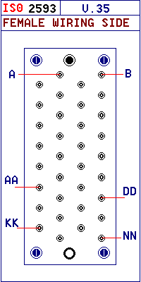
| ISO-2593 assigns the circuits for V.35 on a
34 pin square connector. |
| |
| V.35 Pin Designations |
ISO 2593 |
| CCITT No |
Pin No |
DTE -- DCE |
Description |
| 102 |
B |
---------- |
Signal ground |
| 103 |
P , S |
 |
Transmit data |
| 104 |
R , T |
 |
Receive data |
| 105 |
C |
|
RTS Request to
send |
| 106 |
D |
|
RTS Ready for
sending |
| 107 |
E |
|
DSR Data set
ready |
| 108.1 |
H |
|
DTR Connect data set to
line |
| 109 |
F |
|
Data Channel Receive Line Signal
Detector
(105
is ON at other end) |
| 113 |
U , W |
|
Transmitter signal element timing
from DCE |
| 114 |
Y , AA |
|
Transmitter signal element timing
from DCE |
| 115 |
V , X |
|
Receiver signal element timing from
DCE |
| 141 |
L |
|
Test control |
| 142 |
NN |
|
Test indicator |
|
 |
| |
|
|
| |
|
V.35 describes the modulation methods for 48Kb/s synchronous
full duplex data communication circuits. It also redefines the V.24 circuits
103,104,114 and 115 to make them balanced circuits.The voltage differences
between signal and return wire is +/-0.55 Volts , the remaining circuits are
unbalanced. This interface is used for 56Kb/s and 64Kb/s circuits but is being
replaced by X.21. |
|
| |
|
|
|
|
If you find this useful and have information to add email
Martin Ryan. All contributions ,
queries and constructive criticisms are welcome. |
|